



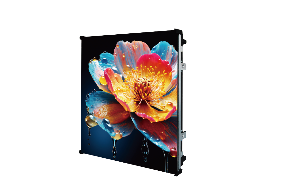
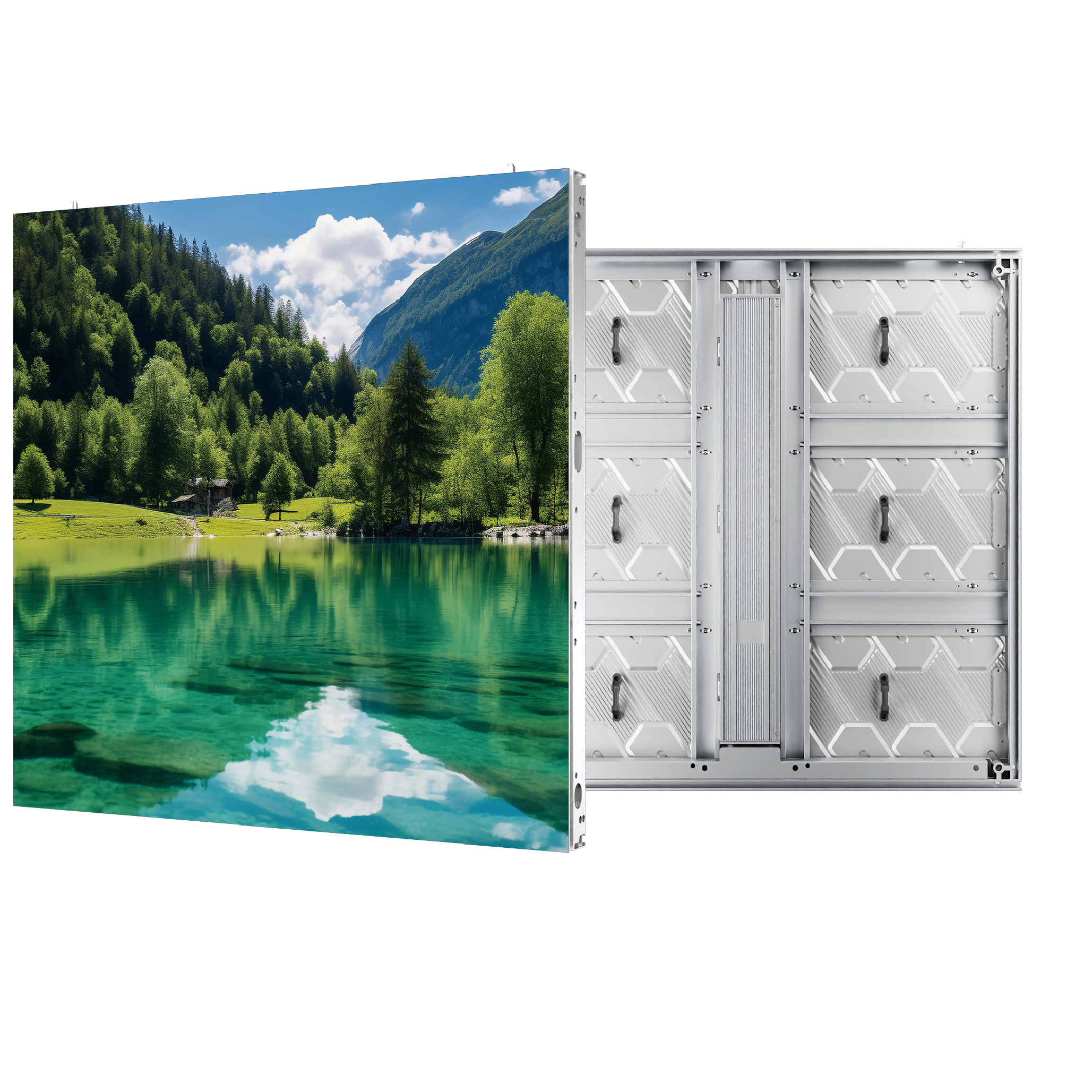
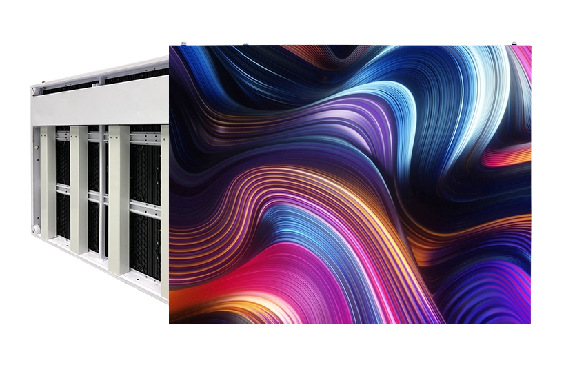
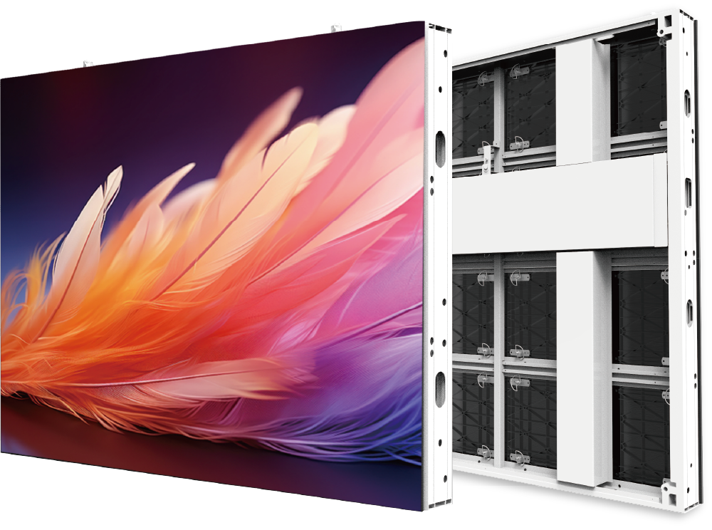
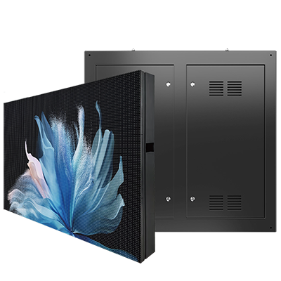
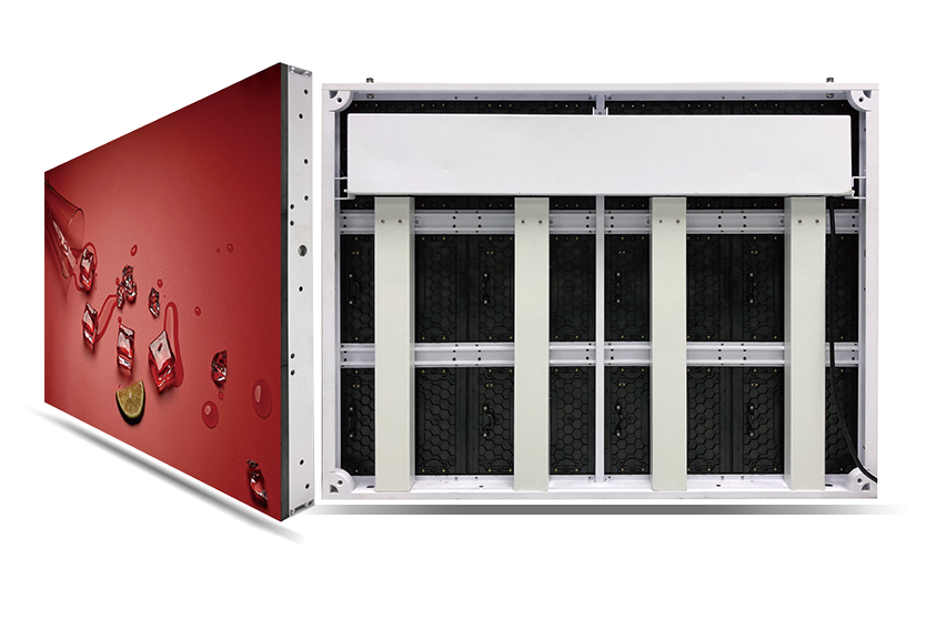
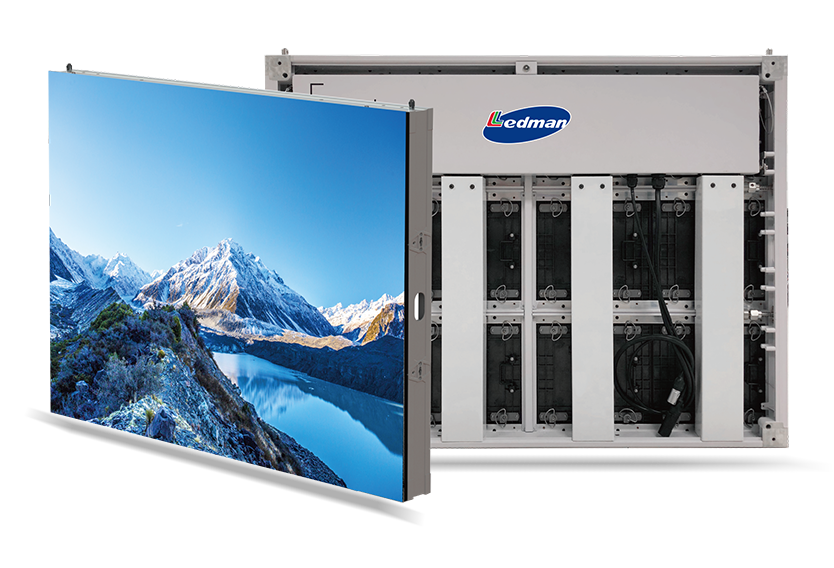
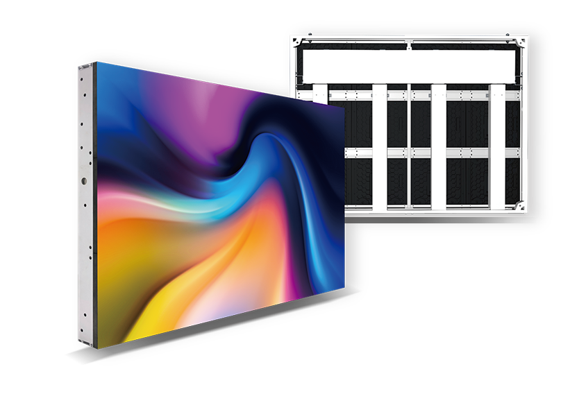
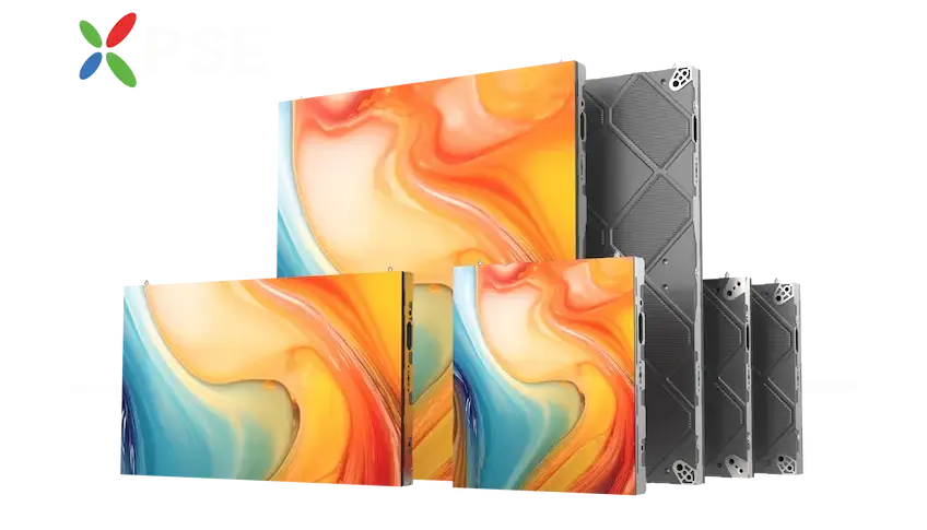
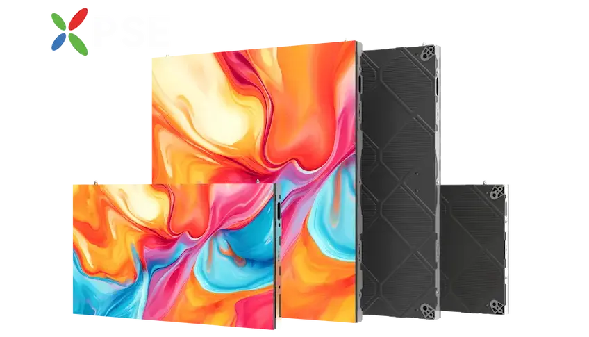
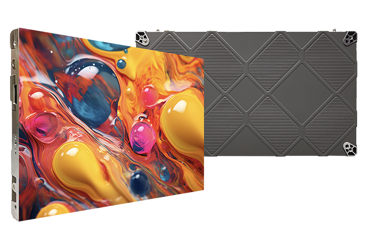
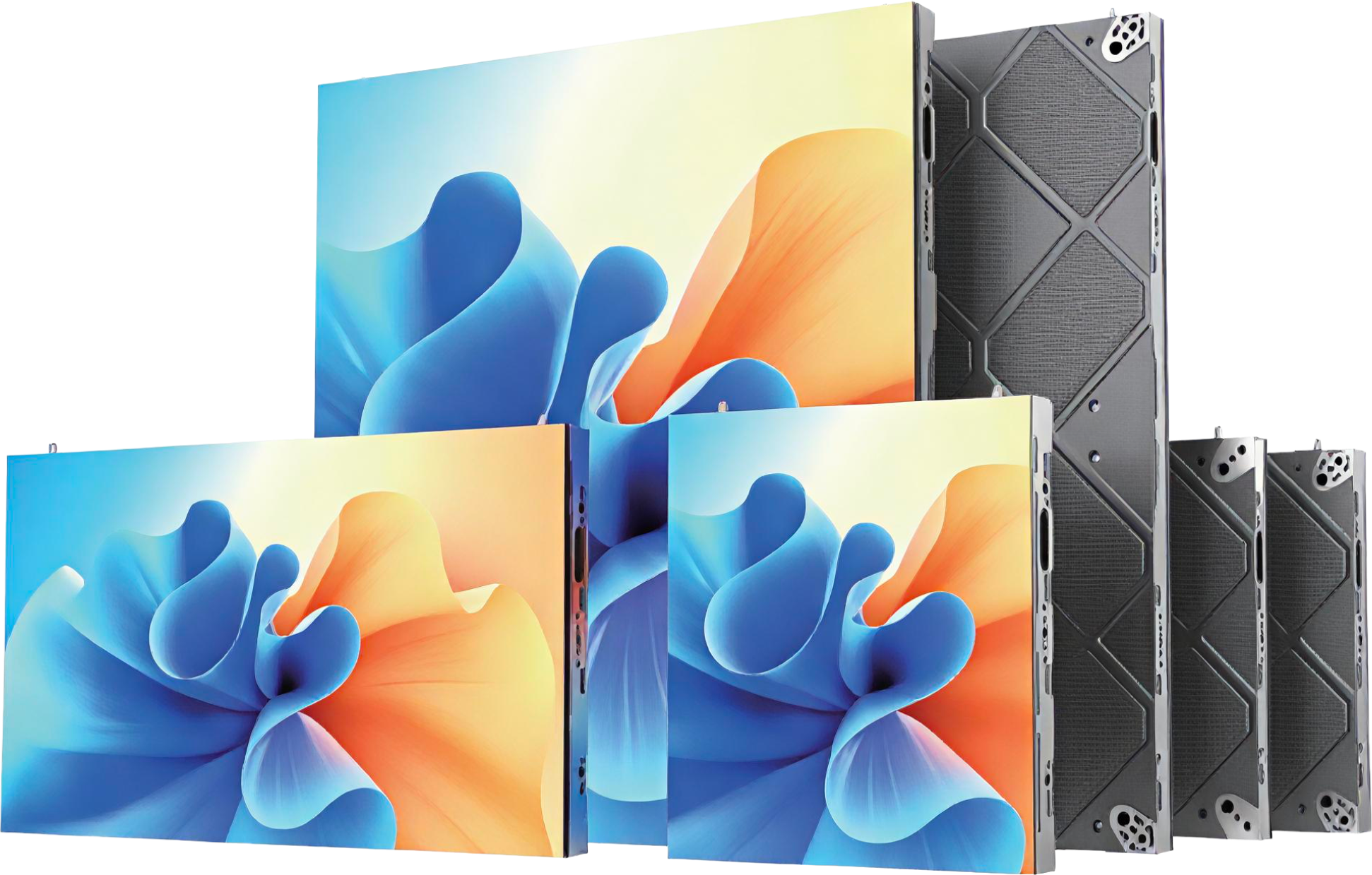
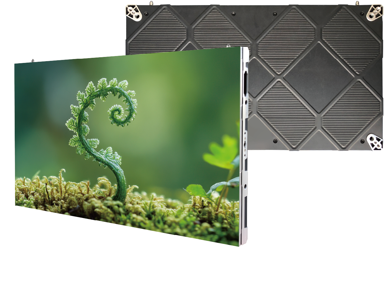
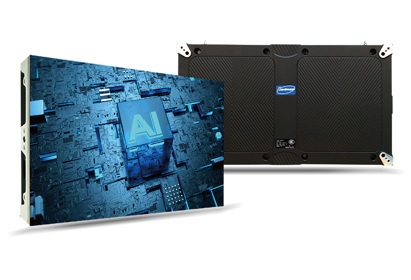
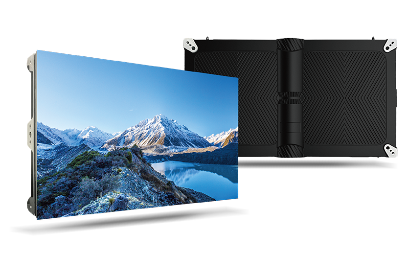
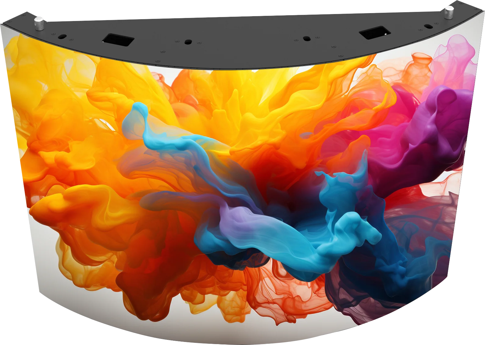
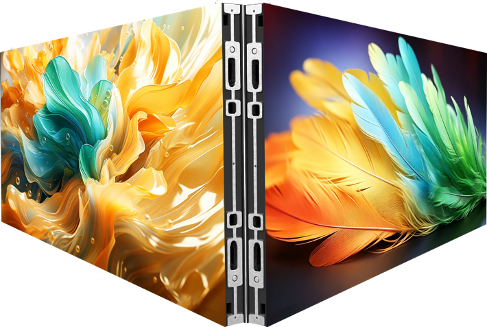
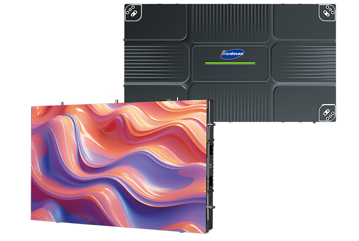
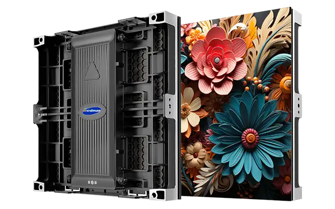



For years, the LED display industry has pursued smaller pixel pitches to increase pixel density and improve image quality. As pixel density has risen, Chip-on-Board (COB) packaging has emerged as the preferred solution for premium UHD LED displays, combining higher reliability with improved optical performance and mechanical durability.
This guide explains how COB LED displays work, the engineering principles behind their performance, the trade-offs compared with other packaging technologies, and the key factors to evaluate when selecting a COB display for different applications.
What Is a COB LED Display?
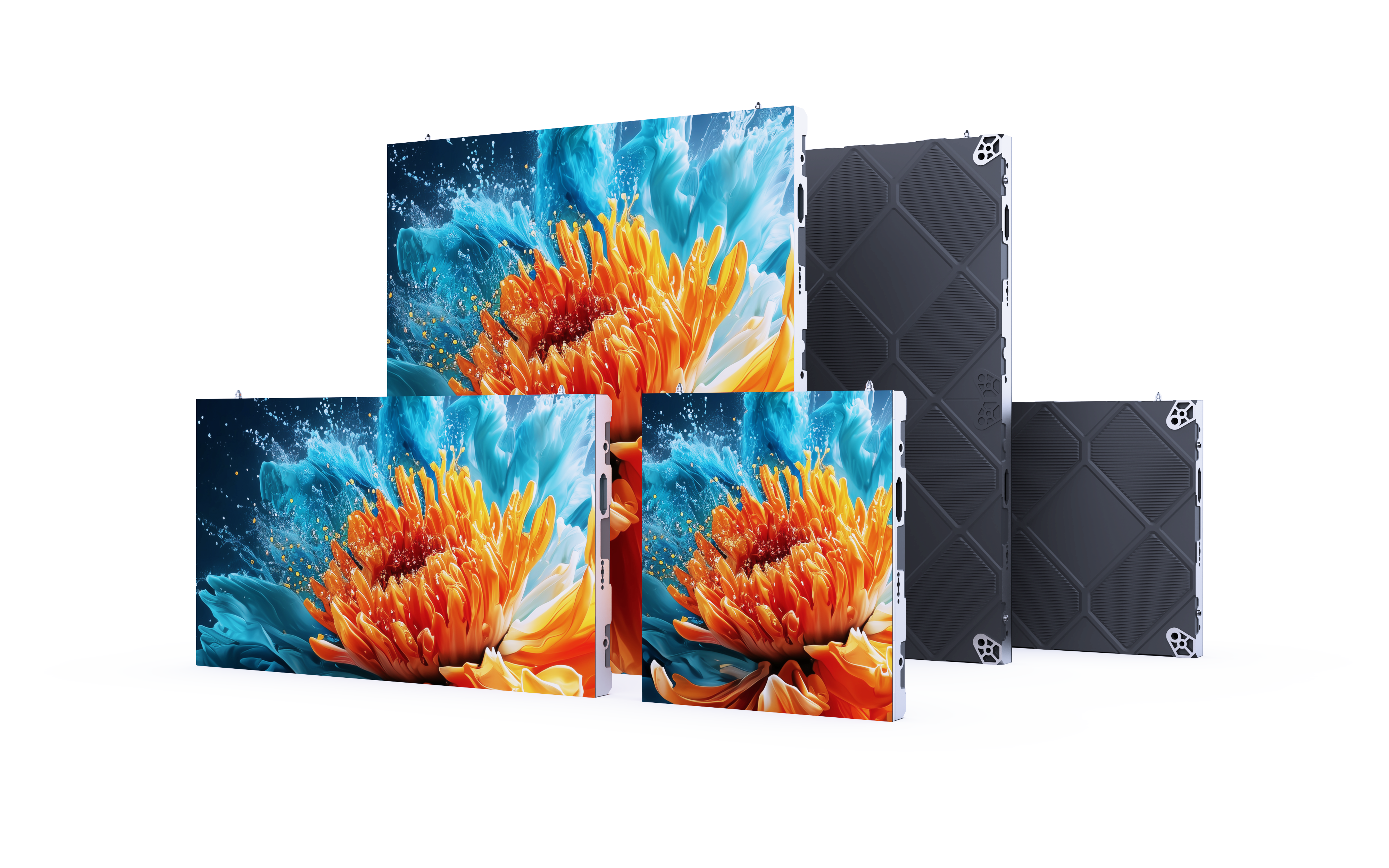
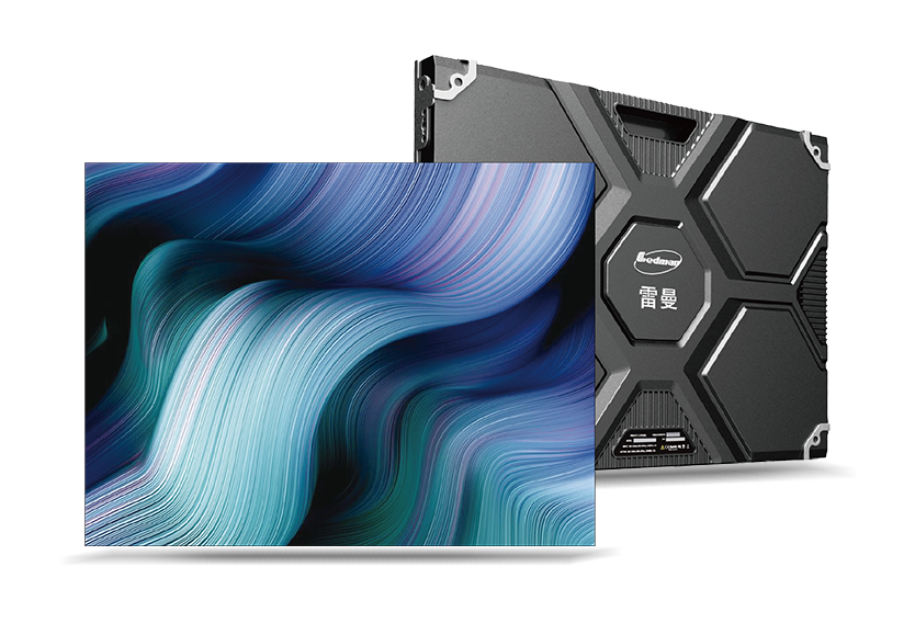
A COB LED display uses Chip-on-Board (COB) packaging, a manufacturing technique in which bare LED chips are mounted directly onto a printed circuit board (PCB) substrate and encapsulated beneath a continuous protective resin layer.
The core engineering advantage lies in eliminating individual LED packages, reducing exposed solder joints, and minimizing the mechanical and environmental failure points commonly associated with conventional SMD displays.
To visualize this technology, imagine a traditional LED display as a grid of thousands of tiny, raised light sources. In contrast, a chip on board LED panel features a flat, smooth, continuous protective surface that helps shield the delicate LED chips from physical impact, dust, and moisture.
How COB Technology Actually Works
Understanding what is chip on board LED packaging requires a closer look at the manufacturing process. Traditional LED packaging first encloses each LED chip inside an individual package before mounting it onto a circuit board. COB eliminates this intermediate packaging step by mounting bare LED chips directly onto the PCB.
- Die Bonding:Bare LED chips are precisely mounted onto the PCB substrate using high-precision automated die-bonding equipment.
- Electrical Interconnection:High-end COB displays typically adopt flip-chip architecture, where LED chips are mounted upside down so that electrical contacts connect directly to the PCB traces without traditional wire bonds. This improves both electrical reliability and thermal performance.
- Resin Encapsulation:The mounted LED array is encapsulated with a specialized epoxy or silicone resin, forming a continuous protective layer across the display surface.
By combining flip-chip architecture with COB LED technology, manufacturers create a shorter and more efficient thermal conduction path, allowing heat to be transferred more effectively into the PCB substrate. Eliminating individual LED packages also enables higher packaging density, making ultra-fine pixel pitches such as P0.9, P0.6, and P0.4 possible while maintaining stable thermal performance and long-term reliability.
COB vs SMD vs GOB vs MIP: The Real Comparison
Choosing the correct display architecture depends on pixel pitch, budget, and environmental conditions. Here is how Chip-on-Board compares against Surface Mount Device (SMD), Glue-on-Board (GOB), and Micro LED in Package (MIP) solutions.
| Feature | Surface Mount Device (SMD) | Glue-on-Board (GOB) | Micro LED in Package (MIP) | Chip-on-Board (COB) |
| Ideal Pixel Pitch | > 1.2 mm | 1.2 mm to 2.5 mm | 0.6 mm to 1.2 mm | < 1.2 mm (P0.9 – P0.4) |
| Physical Protection | Low (exposed lamps) | Moderate (surface glue) | Moderate | High (full encapsulation) |
| Viewing Angle | 140° to 160° | 160° | 160° to 170° | Up to 170°+ |
| Contrast Ratio | Moderate (10,000:1) | Moderate | High | Very High (1,000,000:1) |
| Thermal Path | Longer (through lamp base) | Moderate | Short | Direct to PCB |
| Relative Cost | Baseline | Low-to-Mid | Mid-to-High | Premium |
SMD remains cost-effective for outdoor scoreboards and large indoor video walls viewed from afar.
GOB adds a protective epoxy layer over standard SMD lamps for impact resistance.
MIP acts as a bridge technology that tests micro-LED chips inside tiny individual packages.
However, for ultra-fine-pitch installations demanding uniform visual quality and maximum durability, COB represents the primary engineering choice.
Key Advantages of COB LED Displays
Unmatched Durability and Environmental Protection
Because the entire display module is sealed in epoxy resin, COB screens offer high resistance to physical impacts, dust, moisture, and static electricity. This level of protection makes them ideal for touch-interactive screens, low-hanging video walls, and high-traffic commercial spaces.
Superior Thermal Efficiency and Lower Heat
Direct contact between the LED chip and the PCB substrate drastically reduces thermal resistance. Operating at lower surface temperatures increases diode longevity, reduces color drift over time, and yields measurable energy savings during continuous operation.
Higher Contrast and Ultra-Wide Viewing Angles
Encapsulation materials can be treated with deep black optical coatings. This creates deep black levels, eliminates light leakage, and yields contrast ratios exceeding 1,000,000:1. The flat surface profile also provides horizontal and vertical viewing angles up to 170 degrees without color distortion at extreme angles.
Proven Long-Term Reliability
In mission-critical control centers, operational uptime is essential. Real-world installations demonstrate the maturity of modern COB engineering. For example, LEDMAN installed a fine-pitch COB display array for the Shanghai Bus Group command center that operated for over 8 years with zero component failures and zero maintenance required.
Limitations and Honest Trade-offs
Higher Initial Investment: Advanced manufacturing equipment and cleanroom assembly requirements make fine-pitch COB displays more expensive upfront per square meter than standard SMD panels.
On-Site Service Complexity: Individual light chips cannot be replaced with a standard soldering iron in the field. Module-level swapping or specialized factory calibration equipment is required for repairs.
How to Evaluate a COB LED Display (Buyer’s Checklist)
When reviewing manufacturer specifications, verify these technical factors:
- Pixel Pitch vs. Viewing Distance: Choose the finest pixel pitch that suits your typical viewing distance. For example, a P0.9 display is generally best viewed from around 1 meter away, while a P1.5 display is better suited to viewing distances of about 1.5 meters or more.
- Thermal Management and Surface Temperature: Ask for operating surface temperature data. Lower heat translates directly to longer diode lifespan.
- Color Uniformity and Calibration:Inquire about factory module calibration to prevent patchwork variations across large screens.
- Proprietary Pixel Architectures:Look for advanced energy-saving designs. For instance, LEDMAN utilizes patented Pixel Sharing Engine (PSE) technology to optimize pixel arrangement, reducing power consumption by up to 50% while maintaining crisp 8K resolution.
- Warranty and Field Support:Confirm that the manufacturer provides spare display modules from the same production batch to maintain color consistency during long-term servicing.
Conclusion
Chip-on-Board engineering has shifted expectations for high-resolution video walls. By eliminating discrete packaging and securing chips within a protective matrix, COB delivers high contrast, broad viewing angles, and long-term operating stability. For enterprise environments requiring seamless fine-pitch visual solutions, COB technology represents a durable and future-proof investment.


